Phase Locked Loop Block Diagram
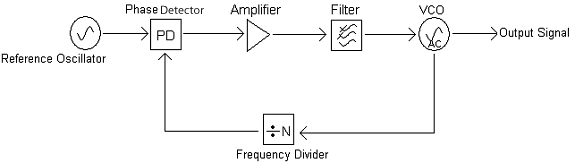
The error signal is then low pass filtered and used to drive a vco which creates an output phase. Phase locked loop system block diagram the figure shows the block diagram of the phase locked loop system in fm transmitter that consists of different blocks such as a crystal oscillator phase detector loop filter voltage controlled oscillator vco and frequency divider.
 Phase Locked Loop Wikipedia
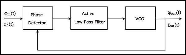
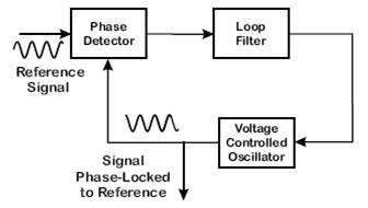
Block diagram and working principle of pll the phase locked loop consists of a phase detector a voltage control oscillator and in between them a low pass filter is fixed.
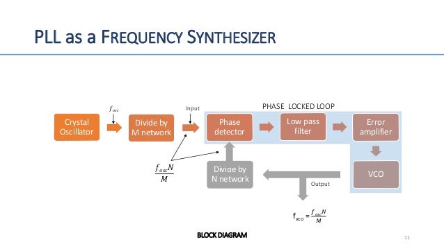
Phase locked loop block diagram. A versatile building block for micropower digital and analog applications 3 cd4046b pll technical description figure 2 shows a block diagram of the cd4046b which has been implemented on a single monolithic integrated circuit. The phase locked loop or pll is an electronic circuit with a voltage controlled oscillator whose output frequency is continuously adjusted according to the input signals frequency. Phase locked loop diagram showing voltages the voltage controlled oscillator vco within the pll produces a signal which enters the phase detector.
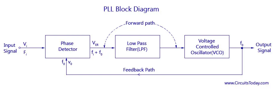
4 cd4046b phase locked loop. Block diagram of a phase locked loop a phase detector compares two input signals and produces an error signal which is proportional to their phase difference. A phase detector basically a comparator which compares the input frequency fiwith the feedback frequency fo the phase detector provides an output error voltage ver fifowhich is a dc voltage.
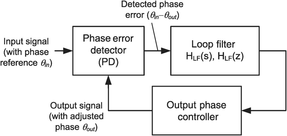
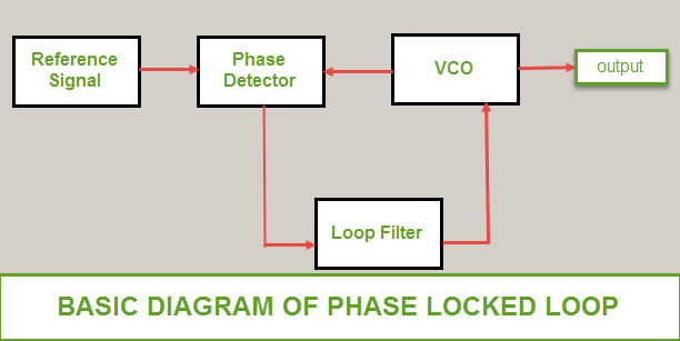
A phase locked loop is used for tracking phase and frequency of the input signal. It is a very useful device for synchronous communication. Here the phase of the signals from the vco and the incoming reference signal are compared and a resulting difference or error voltage is produced.
The input signal vi with an input frequency fi is conceded by a phase detector. What is phase locked loop. Figure 1 shows a simplified block diagram of the major components in a pll.
The pll structure consists of a low power linear vco and two. Block diagram phase locked loops the input signal vi with an input frequency fi is passed through a phase detector. A phase locked loop pll is a closed loop frequency control system based on the phase difference between the input clock signal and the feedback clock signal of a controlled oscillator.
Phase locked loops are the circuits used to maintain synchronization between input and output frequency of oscillator circuits by comparing the difference in phase of the two signalswith the evolution of ic it has emerged as the basic building block of electronic circuits.
 Block Diagram Of A Phase Locked Loop Courtesy
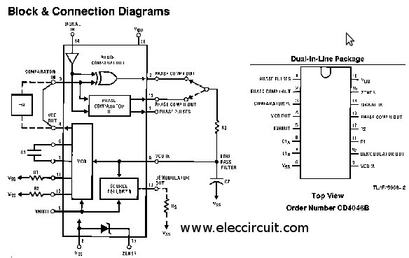 Ic 4046 Datasheet Phase Locked Loop
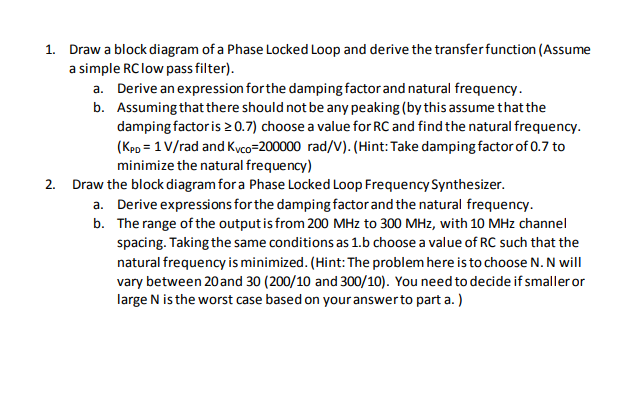 Solved Draw A Block Diagram Of A Phase Locked Loop And De
 Basics Of Phase Locked Loop Techniques Chapter 4
 Phase Locked Loop Fbswiki
 Block Diagram Of The Phase Locked Loop Circuit Download
 Figure 2 From Stability And Resolution Analysis Of A Phase
 Figure 2 24 From Delay Flip Flop Dff Metastability Impact
 Phase Locked Loop Design And Construction Elliot Nwaobi
 Phase Locked Loop Block Diagram Download Scientific Diagram
 Basics Of Pll I Operation I Block Diagram Eeeguide Com
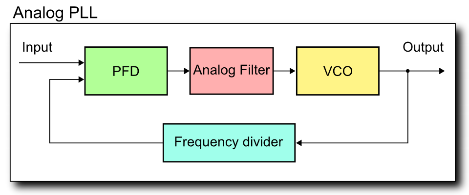
File Analog Pll Block Diagram Png Wikimedia Commons
 50 Ghz Phase Locked Loop Block Diagram Download
 Phase Locked Loop Operating Principle And Applications
 Phase Locked Loop
 Phase Locked Loop Basics Pll
 1 Block Diagram Of A Phase Locked Loop Download
 Phase Locked Loop Ic Tutorialspoint
 Compare Phase Locking Methods Of Rf Sources Microwaves


 Phase Locked Loop Mini Projects Electronics Tutorial
 Vhf Community Radio Electronics An Introduction
 Explain Pll Using Block Diagram Of Ic 565
Belum ada Komentar untuk "Phase Locked Loop Block Diagram"
Posting Komentar